Samsung Develops First 50nm DRAM Chip
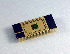
Samsung Electronics Co., Ltd., the world leader in advanced memory technology, announced today that it has developed the industry’s first 50-nanometer (nm) DDR2 DRAM (dynamic random access memory) chip, which will increase production efficiency from the 60nm level by 55 percent. The new 1-gigabit (Gb) DRAM incorporates advanced technologies such as three-dimensional (3D) transistor design and multi-layered dielectric technology, which greatly enhance performance and data storage capabilities.
“With the 50nm DRAM development, we’re continuing our technology leadership, paving the way for our customers to reap not only greater cost efficiencies but also to make superior products,” said Nam Yong Cho, executive vice president of memory sales & marketing at Samsung Electronics’ Semiconductor business.
Key to the exceptional production efficiencies in the newly developed 50nm process is the use of a selective epitaxial growth transistor (SEG Tr). This 3D transistor has a broader electron channel that optimizes the speed of each chip’s electrons to reduce power consumption and enable higher performance.
Continued miniaturization of the overall memory circuit and an increasingly limited area of coverage within a wafer cell make it much harder to secure and sustain sufficient volumes of electrons. Adding to the 50nm design improvements, the SEG transistor introduces a multi-layered dielectric layer (ZrO2/Al2O3/ZrO2) to resolve weak electrical features. In addition, the new dielectric layer sustains higher volumes of electron to increase storage capacity, ensuring higher reliability in storing data.
Further, Samsung’s proprietary RCAT (Recess Channel Array Transistor) technology - a fundamental 3D transistor technology which received the best paper award at the VLSI symposia in 2003 - also has been adapted to work well with Samsung’s 50nm DRAM process. The RCAT, which effectively doubles the refresh term of DRAM, is a critical technology supporting higher scalability for DRAM regardless of chip size ? a key feature for enabling circuitry beyond 50nms.
The 1 Gb 50nm chip encompasses three generations of DRAM technology (70nm, 60nm and 50nm) in achieving the most advanced level yet for DRAM mass production.
Samsung’s new 50nm process technology can be applied to a broad range of DRAM chips including graphics and mobile DRAM. With mass production slated for 2008, the 50nm DRAM chip is well positioned to become the mainstay of a DRAM market that is expected to account for US $55 billion by 2011.
Source: Samsung


