March 30, 2020 feature
Resolving spatial and energetic distributions of trap states in metal halide perovskite solar cells

Thamarasee Jeewandara
contributing writer

In a new report published on Science, Zhenyi Ni and a research team in applied physical sciences, mechanical and materials engineering and computer and energy engineering in the U.S. profiled spatial and energetic distributions of trap states or defects in metal halide perovskite single-crystalline polycrystalline solar cells. The researchers credited the of metal halide perovskites (MHPs) to their high , , and (representing disorder in the system). Theoretical studies have demonstrated the possibility of forming deep charge traps at the material surface due to low formation energy, structural defects and grain boundaries of perovskites to guide the development of passivation techniques (loss of chemical reactivity) in . Charge trap states play an important role during the degradation of perovskite . Understanding the distribution of trap states in their space and energy can clarify the impact of charge traps (defects) on charge transport in perovskite materials and devices for their optimal performance.
Scientists have broadly used (TAS) and thermally stimulated current (TSC) methods to measure the energy-dependent trap density of states (tDOS) . The methods can generally reach a trap depth approximating 0.55 eV—deep enough to make efficient solar cells. To that exist within wide-band gap perovskites, researchers have used techniques such as and sub-band gap photocurrent. However, most techniques cannot be applied to already completed solar devices to measure the spatial distribution of trap-states. In this work, Ni et al. demonstrated the drive-level capacitance profiling method (DLCP) – an alternate -based technique to provide well-characterized spatial distributions of carrier and trap-densities in perovskites. The scientists mapped the spatial and energetic distribution of trap-states within perovskite single crystals and polycrystalline thin films for straightforward comparison.

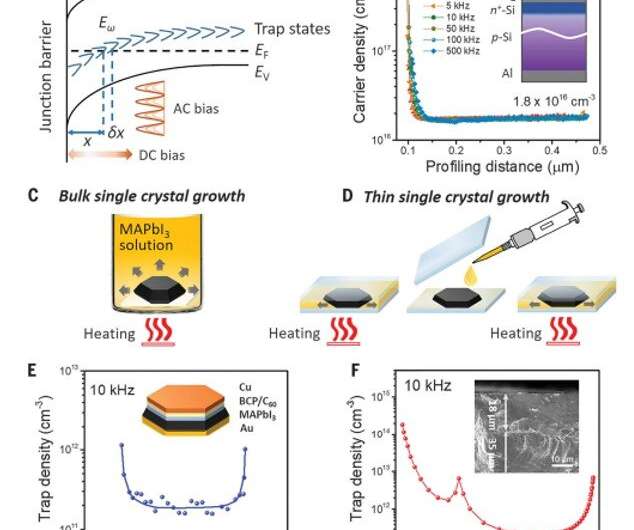
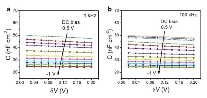
The team developed the DLCP (drive-level capacitance profiling) method to study the spatial distribution of defects in the band gap of amorphous and polycrystalline semiconductors such as . The method could directly determine the carrier density to include both free carrier density and trap density within the band gap of semiconductors as well as their distribution in space and energy. They estimated the trap density by subtracting the estimated free carrier density measured at high alternating current (ac) frequencies from the total carrier density measured at low ac frequency. The technique allowed the team to derive the energetic distribution of trap states. To validate the accuracy of the carrier density measured using the DLCP method, the scientists performed DLCP measurements on a silicon solar cell fabricated on a p-type crystalline Si (p-Si) wafer with a n-type diffusion layer Si (n+) on top. The measurement was consistent with the dopant concentration of the p-Si wafer obtained from the conductivity measurement to validate the accuracy of the carrier density measured using DLCP.
To profile the carrier and trap densities using DLCP, the researchers investigated across a device from one electrode to the counter-electrode to understand the location of junctions in planar-structured perovskite solar cells. The team conducted several experiments and observed that perovskite cells typically maintained a n+-P junction between device constituents. In order to determine the profile depth corresponding to the physical material depth, Ni et al. constructed a device containing a double-layer of (MAPbI3) thin crystals to locate the charge traps. When they profiled the trap density of the engineered device, they obtained a peak in the trap density at a profiling distance of 18 µm.
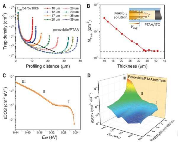
![Spatial distributions of trap states in a MAPbI3 thin single crystal. (A) Dependence of the carrier density on the profiling distance of a 39-mm-thick MAPbI3 thin single crystal at different ac frequencies, as measured by DLCP. (B) Dependence of the trap density on the profiling distance of a MAPbI3 thin single crystal measured at an ac frequency of 10 kHz. The carrier density measured at 500 kHz is regarded as free carriers. (C) Schematics of a MAPbI3 thin single crystal on a PTAA/ITO substrate before mechanical polish, after mechanical polish, and after oxysalt [(C8–NH3)2SO4] treatment. (D) Trap density near the junction barrier of a MAPbI3 thin single crystal before mechanical polish, after mechanical polish, and after oxysalt treatment. Credit: Science, doi: 10.1126/science.aba0893 Resolving spatial and energetic distributions of trap states in metal halide perovskite solar cells](https://scx1.b-cdn.net/csz/news/800a/2020/2-resolvingspa.jpg)
The team then studied the trap distribution in perovskite single-crystal solar cells and observed the highest power conversion efficiency (PCE) of solar cell to be only 17.9 percent; far lower than that of polycrystalline solar cells. They were unaware of the underlying mechanism that limited carrier diffusion in thin crystals and conducted DLCP measurements to investigate the relationship of trap density and trap distributions using synthetic-crystal methods. The team observed the spatial distribution of carrier densities throughout a typical MAPbI3 thin single crystal, which they synthesized using a space-confined growth method at different frequencies, and noted increasing carrier density with decreasing ac frequency, indicating the existence of charge traps in the MAPbI3 thin single crystal.

To understand the origin of deep trap density at the perovskite interface, the team used and examined perovskite samples of different compositions. They compared trap density distributions between perovskite single crystals and polycrystalline thin films with varying compositions. The trap density distributions for thin single crystals were several orders of magnitude lower than that in polycrystalline thin films. The results showed the importance of adequate surface modification processes to reduce trap densities in perovskite single crystals at the interface of polycrystalline thin films to enhance device performance. The results point toward an important direction to boost the performance of perovskite solar cells and other electronic devices by reducing the trap density at the interface.
![Spatial and energetic distributions of trap states in perovskite thin films. (A) J-V curve of the Cs0.05FA0.70MA0.25PbI3 thin-film solar cells. The inset shows the device structure. (B) Dependence of the trap density on the profiling distance for the perovskite thin film in the solar cell measured at an ac frequency of 10 kHz. (C) tDOS of the perovskite thin-film solar cell, as measured by the TAS method. (D) Spatial and energy mapping of the densities of trap states of the perovskite thin film in the solar cell, as measured by DLCP. (E) Cross-sectional HR-TEM image of the stack of perovskite and PTAA. The dashed squares mark the areas where the fast Fourier transforms of the lattices were performed, with white and yellow indicating zone axes of [1 −1 −1] and [2 1 0], respectively. The red lines denote the orientation of the facets. (F) Fast Fourier transforms of the areas indicated in (E). (G) Measured and simulated J-V curves of planar-structured solar cells based on MAPbI3 polycrystalline thin films. The thin-film (single crystal) bulk and interface trap densities were adopted for the simulations. (H) Dependence of the PCE of the MAPbI3 thin-film solar cell on the bulk and interface trap densities. The dashed lines denote the contour lines of certain PCE values, which are noted. Credit: Science, doi: 10.1126/science.aba0893 Resolving spatial and energetic distributions of trap states in metal halide perovskite solar cells](https://scx1.b-cdn.net/csz/news/800a/2020/4-resolvingspa.jpg)
In this way, Zhenyi Ni and colleagues used the solar cell capacitance simulator to simulate the thin-film and single-crystal perovskite solar cells with varying trap densities. The range of traps measured with DLCP measurements were deep enough to predict the behavior of solar cells and reduce the bulk trap density of materials and increase the power conversion efficiency (PCE) up to 20 percent. By decreasing the interface trap density, they increased the PCE values closer to the PCE observed for a trap-free thin film solar cell. The data simulated for single-crystal solar cells , showing that the PCE of the single-crystal solar cell could be further improved at the device interface to harvest more sunlight.
Written for you by our author —this article is the result of careful human work. We rely on readers like you to keep independent science journalism alive. If this reporting matters to you, please consider a (especially monthly). You'll get an ad-free account as a thank-you.
More information: Zhenyi Ni et al. Resolving spatial and energetic distributions of trap states in metal halide perovskite solar cells, Science (2020).
James M. Ball et al. Defects in perovskite-halides and their effects in solar cells, Nature Energy (2016).
Qi Jiang et al. Surface passivation of perovskite film for efficient solar cells, Nature Photonics (2019).
Journal information: Science , Nature Energy , Nature Photonics
© 2020 Science X Network


