September 2, 2021 feature
Materials for superconducting qubits

Thamarasee Jeewandara
contributing writer
 False color optical image of a representative transmon qubit from our study. Niobium regions include the center-pin of the coplanar waveguide resonator (green), the transmon capacitor pads (purple), and the ground plane (gray). The aluminum Josephson junction is shown in white. Black areas indicate where the metal has been etched away, and the sapphire substrate is exposed. (b) Effective circuit diagram of a transmon qubit coupled to a resonator. Each circuit element is schematically colored as in (a). The resonator is comprised of a center-pin coupled to ground via a capacitor (Cr) and an inductor (Lr). EJ and C refer to the Josephson energy and the capacitance of the qubit respectively. The qubit is capacitively coupled to the center-pin of the resonator (Cc) and to ground (Cg). (c) Measured relaxation times (T1) for three rounds of devices fabricated with sputtered (purple circles), HiPIMS optimized (blue diamonds), and HiPIMS normal (green squares) niobium films, for a total of nine devices. Error bars indicate standard deviation across all T1 measurements taken on a particular device. Credit: Communications Materials, 10.1038/s43246-021-00174-7")
The connection between microscopic material properties and qubit coherence are not well understood despite practical evidence that material imperfections present an obstacle to applications of . In a new report now published on Communications Materials, Anjali Premkumar and a team of scientists in electrical engineering, nanomaterials, physics and angstrom engineering at Princeton University and in Ontario, Canada, combined measurements of (T1) times with spectroscopy, alongside microscopy of (Nb) films used during qubit development. Based on films deposited via three different techniques, the team revealed correlations between transmon qubit relaxation times and intrinsic film properties, including grain size to enhance oxygen diffusion along grain boundaries, while also increasing the concentration of suboxides near the surface. The residual resistance ratio of the polycrystalline niobium films can be used as a figure of merit to understand qubit lifetimes, and the new approach charts a path for materials-driven improvements of superconducting qubit performance.
Superconducting qubit materials
In this work, Premkumar et al. bridged the gap between qubit performance and microscopic materials, based on a materials-and-device specific investigation of transmon qubits. Superconducting qubit technology is a promising platform for fault-tolerant quantum computation. Scientists have achieved significant enhancements in qubit coherence through new device designs and improved fabrication processes. Nevertheless, the performance improvements have started to plateau since are not well understood. As a result, in order to understand methods of limiting loss mechanisms in qubit materials. Many studies have surfaces and interfaces during the decoherence of transmon qubits, including proposed mechanisms that involve interactions between . To understand the phenomena, a scope of multidisciplinary research is required to investigate the relevant material properties and their connections with qubit performance. Premkumar et al. used spatially resolved and microscopy to characterize the structural and electronic properties of niobium thin films used in transmon qubit devices. The team detailed the mechanisms underlying the observed microscopic features to resistance and relaxation times. The results form a critical step to connect precise materials properties with microscopic models to improve qubit performance.
 of the Nb films with varying photon energy. (a) Representative PES spectrum of the Nb 3d3/2 and 3d5/2 core levels, measured on the sputtered film for a photon energy (hν) of 3330 eV (black dots) and fit with five components. (b) Measured spectra for all three film types at 3330 eV, normalized to the intensity of the Nb2O5 component. For each film, the measured intensity of the Nb (c) and Nb2O5 (d) peaks are plotted at several photon energies. The sum of the signals from the different oxidation states in a given film is normalized to one, and the error bars show a 1% error, as estimated from the signal-to-noise of measured data. The intensity of Nb and Nb2O5 increase and decrease with energy, respectively, indicating the presence of a surface oxide layer. Credit: Communications Materials, 10.1038/s43246-021-00174-7")
Qubit design and performance
The team performed qubit characterization on transmon qubits that are typically for quantum computing and . The transmon qubit design includes a with a thin aluminum oxide barrier between the superconducting wires shunted by a large capacitor to . Scientists can control the transmons in a circuit quantum electrodynamics platform and at the resonator frequency, as a function of qubit state. During the study, Premkumar et al. used three different deposition methods to deposit the niobium film and fabricate the transmon devices. First, they deposited the materials on sapphire substrates and used direct current sputter deposition for superconducting qubit fabrication. They then used two other methods including high-power impulse magnetron sputtering (HiPIMS) and optimized the technique to and develop denser films. The scientists then characterized the dependence of qubit performance on deposition techniques using relaxation measurements (T1). The results showed a clear statistical difference between the three deposition techniques, where the sputtered niobium consistently performed the best, followed by the optimized HiPIMS method and then the normal HiPIMS method. The team used a range of characterization methods to study the films and understand the possible microscopic origins of the coherence differences.
-
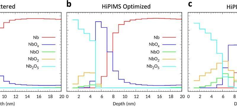
Depth profiles of the different oxidation states of Nb. The profiles for the sputtered (a), HiPIMS optimized (b), and HiPIMS normal (c) Nb films were reconstructed from PES data using a maximum-entropy method algorithm. Each film shows a surface layer of a few nm of Nb2O5, a transition layer with varying concentrations of different suboxides, and the Nb metal bulk. In particular, the HiPIMS normal film shows significant concentrations of NbO and NbO2 in the transition layer and deeper penetration of NbOx into the metal. Credit: Communications Materials, 10.1038/s43246-021-00174-7 -
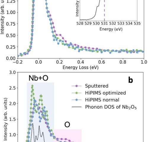
Resonant inelastic X-ray scattering (RIXS) spectra measured for the Nb films. a RIXS measurements at the oxygen K-edge resonance for an incident energy of 531 eV. The inset shows the O-K absorption spectrum of the sputtered film with a vertical dashed line at the resonance. b Close-up view of the RIXS spectra after subtraction of the elastic line, with the phonon density of states (DOS) calculated for Nb2O5 from45. The overall scaling factor of the DOS was chosen to aid visualization. The DOS was reported to arise from both niobium and oxygen up to ≈70 meV, and mostly from oxygen at higher energies, as represented by the blue and pink bands, respectively. The lower intensity at higher energies for the HiPIMS films indicates a larger concentration of oxygen vacancies. Credit: Communications Materials, 10.1038/s43246-021-00174-7
Understanding the surface material
To understand the surface oxides on the three types of Nb films, Premkumar et al. used a combination of methods such as soft and hard x-ray photoemission spectroscopy and resonant inelastic x-ray scattering. All three film types showed (Nb2O5) to be the main constituent. The sputtered film contained the sharpest oxide-metal interface, followed by the HiPIMS optimized method and the HiPIMS-normal film deposition technique. The scientists also used resonant inelastic x-ray scattering to achieve sensitivity to low-energy excitations of the electronic structure. They then correlated the surface oxide findings with surface morphology and grain size using , and measurements for all three types of Nb films. The near-surface morphology of the HiPIMS-normal film was visibly different, where the oxide layer adhered to lower grains. The electron-energy loss spectra provided an outlook of chemical properties near the surface of the oxide-metal, while transmission electron microscopy highlighted the grain boundaries of each sample and atomic force microscopy indicated further information about the grain morphology and size.
–(c) show high-angle annular dark-field scanning transmission electron microscopy (HAADF-STEM) measurements at cross-sections of the films' surfaces, revealing a ≈ 5 nm oxide layer and variations in grain size. Panels (d)–(f) show O-K-edge electron-energy loss spectroscopy (EELS) spectra measured at the locations indicated on the HAADF-STEM images. For the sputtered and HiPIMS optimized films, both the EELS spectra within a grain (left) and the spectra taken along a grain boundary (right) show a transition from a double peak (Nb2O5) to a single peak (suboxides) to a negligible peak (metal). However, for the HiPIMS normal film, EELS spectra along the grain boundary reveal similar oxidation peaks to the surface oxide layer, indicating that oxygen has diffused into the grain boundary to form oxides. Panels (g)–(i) show TEM bright-field images of cross-sections of the films' surfaces, where the white dotted lines delineate grain boundaries for the sputtered and HiPIMS optimized films, and the yellow arrow points to a gap at the grain boundary for the HiPIMS normal film. The grainy, light gray layer above the surface is platinum, which protects the surface during sample preparation. Panels (j)–(l) show atomic force microscopy (AFM) images measured over a 500 nm x 500 nm area. It is visually evident that the sputtered film grain size is the largest, and the HiPIMS normal film grain size is the smallest. Credit: Communications Materials, 10.1038/s43246-021-00174-7")
Outlook
In this way, Anjali Premkumar and colleagues noted a clear correlation between the qubit relaxation times (T1) and the characterization of Nb (niobium) films, including the residual resistance ratio, grain size and surface suboxide concentration. The team found the total qubit relaxation time to be the sum of multiple mechanisms; where the Nb films deposited by varied techniques dominated the outcomes. The study therefore established a significant link between the performance of superconducting transmon qubits and materials properties during qubit fabrication. The work investigated the microscopic variations among Nb thin films deposited using three different sputtering methods, to specifically understand the grain size, suboxide integration and penetration at the oxide-metal interface, and suboxide intragrain concentration near the surface. The outcomes of this study form a solid basis to develop physical models that can guide the development of materials for superconducting qubits.
Written for you by our author —this article is the result of careful human work. We rely on readers like you to keep independent science journalism alive. If this reporting matters to you, please consider a (especially monthly). You'll get an ad-free account as a thank-you.
More information: Anjali Premkumar et al, Microscopic relaxation channels in materials for superconducting qubits, Communications Materials (2021).
R. Barends et al, Coherent Josephson qubit suitable for scalable quantum integrated circuits, �鶹��Ժical Review Letters (2013).
A. Place et al, New material platform for superconducting transmon qubits with coherence times exceeding 0.3 milliseconds, Nature Communications (2021).
Journal information: �鶹��Ժical Review Letters , Nature Communications
© 2021 Science X Network


