July 30, 2020 feature
Epitaxial antiperovskite/perovskite heterostructures for materials design

Thamarasee Jeewandara
contributing writer

Engineered or layered materials made with complex oxide materials are a rich source of and applications. Materials scientists aim to develop new materials functionalities by interfacing with substrates containing dissimilar crystallographic properties, in a vastly unexplored avenue. In a new report, Camilo X. Quintela and an international group in materials science, physics and engineering in the U.S., Norway, China and South Korea proposed an unprecedented direction for materials design based on and oxide perovskite crystals. In this work, they successfully layered two crystalline materials known as perovskites and antiperovskites together, to create an interface with unique electrical properties for applications in a new class of quantum materials.
During the experiments, Quintela et al. developed sharp interfaces between the nitride antiperovskite and oxide perovskites such as and (SrTiO3). Then using spectroscopic techniques and first-principles calculations, they noted a coherent interfacial monolayer merge between the two antistructures and surprisingly mediate the antiperovskite/perovskite heterointerface beyond theoretical predictions. The results will assist develop exciting new properties at the interface for ultra-low-power applications in , such as , and storage devices. The work is now published in Science Advances.
![HAADF-STEM images of the Mn3GaN/LSAT interface and corresponding recorded EDS. (A) and (B) [100]-projected HAADF-STEM images of the Mn3GaN/LSAT interface and (below each image) corresponding recorded EDS data along the atomic rows represented by yellow arrows in the HAADF-STEM image. EDS line profiles across the interface show a dominant Mn signal at the interface. Overlaid on the HAADF-STEM images is the proposed atomic configuration at the interface based on EELS and EDS analyses. Credit: Science Advances, doi: 10.1126/sciadv.aba4017 Epitaxial antiperovskite/perovskite heterostructures for materials design](https://scx1.b-cdn.net/csz/news/800a/2020/1-epitaxialant.jpg)
Perovskite and antiperovskite crystals
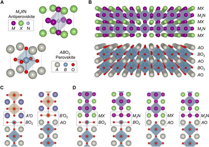
Perovskite crystals are usually oxides with positively and negatively charged ions with promising optical, magnetic and electrical properties. In antiperovskites the placement of the positively and negatively charged ions are flipped to create another class of materials with different properties to perovskites. Antiperovskite materials are intermetallic materials with perovskite crystal structure and much like their oxide perovskite counterparts they show a variety of tunable physical properties including , , and topological electronic behavior. Among such anti-perovskite materials, -based nitride compounds, denoted M3XN, where M equals transition metal and X equals metallic or semiconducting elements, are particularly interesting, with high sensitivity to Such materials sensitivities result from strong spin-lattice coupling characteristics of M3XN compounds, which can be tuned or manipulated through . Additionally, scientists have used the physical properties of as external triggers to tune the functionality of antiperovskite materials. The ABO3 compounds are unrivalled material systems to interface with M3XN nitride antiperovskites due to their analogous structures, to promote (the assembly of dissimilar materials into a single film). To explore epitaxy at the atomic level, Quintela et al. investigated the interfacial structure and chemistry between nitride antiperovskite and oxide perovskite materials.
Developing and characterising the nitride antiperovskite/oxide perovskite interface
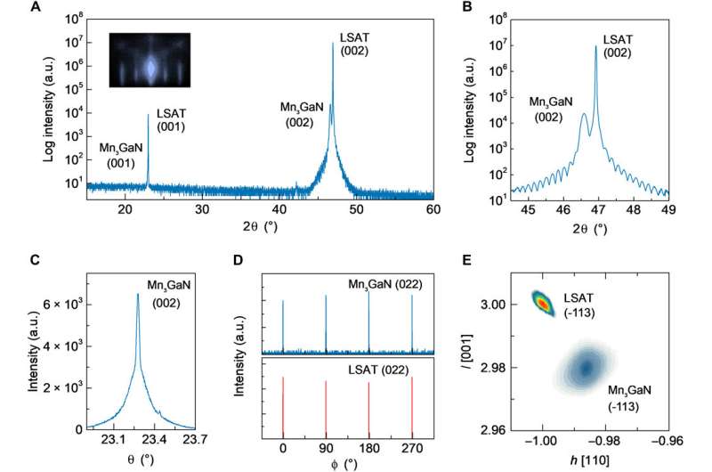
In this work Quintela et al. fabricated a high-quality Mn3GaN film on (La0.3Sr0.7)(Al0.65Ta0.35)O3 (abbreviated LSAT) and strontium titanate single-crystal substrates as paradigms of M3XN/ABO3 interfaces. Using (XRD), they structurally characterized the 60-nm thick Mn3GaN film grown on the LSAT substrate and monitored the epitaxial growth and single-phase structure of the films using (RHEED). The results showed the high crystalline quality of the film and the pristine interface.

To understand the structure and chemical composition of the Mn3GaN/LSAT interface, Quintela et al. combined scanning transmission electron microscopy (STEM) with (EELS) and (EDS). The first interfacial Mn3GaN monolayer showed a pattern of alternating bright and dark spots to indicate compositional or structural reconfiguration at the interface. Using simulations and structural chemical analyses, the team showed transitions from the LSAT substrate to the Mn3GaN film mediated through a sharp interfacial monolayer. To determine the atomic structure of this interfacial monolayer, Quintela et al. performed additional STEM and EDS studies and showed the ordering of atoms in a two-dimensional (2-D) periodic structure with rotational symmetry.
First-principles calculations
The team performed first-principles calculations to study the stability of the interfacial model derived from atomic resolution experiments. Using simulations, they calculated the formation energies to test for stability and confirmed the interfacial model to be energetically stable. Additional work, however, showed apparent discrepancies between the experimental and theoretical studies, which the scientists credited to the onset of Mn3GaN growth in the presence of an energy barrier, where the discrepancy prevented the system from relaxing from the local to the global energy minimum. Quintela et al. further explored this hypothesis in their work. The combined experimental and theoretical studies showed how the interfacial monolayer worked as a structural bridge between the perovskite substrate and antiperovskite film to establish between the (dissimilar crystal structure) materials with different chemical composition and binding.
![Illustration of the Mn3GaN/LSAT heterointerface based on our experimental results. (A) Schematic [100] perspective view of the Mn3GaN/LSAT heterointerface. Orange line in layer 2 is a guide to the eyes, showing buckling of the Mn and Ga atoms. (B) Representation of the Mn3GaN/LSAT heterointerface as a stacking of atomic unit cell planes. (C) [001] projections of the MnN interfacial layer (top image) and MnN layer overlaid with the (Al/Ta)O2 LSAT termination layer (bottom image). Dashed square represents the interfacial MnN unit cell. Credit: Science Advances, doi: 10.1126/sciadv.aba4017. Epitaxial antiperovskite/perovskite heterostructures for materials design](https://scx1.b-cdn.net/csz/news/800a/2020/3-epitaxialant.jpg)
In this way, Camilo X. Quintela and colleagues realized an atomically sharp bridging structure as an epitaxial interface between the nitride antiperovskites and oxide perovskites for the first time. The work forms a critical step to develop a new class of epitaxial heterostructures using materials with dissimilar crystallochemical properties. The potential to engineer novel heterointerfaces provides an exciting playground to manipulate interfacial physical properties and establish new states of matter. Due to the of these materials, which includes , the rational design of epitaxial heterostructures of antiperovskites and perovskites is of great importance for property tuning and functional device design. The team envision that this strategy will open a new and exciting chapter for materials design and engineering.
Written for you by our author —this article is the result of careful human work. We rely on readers like you to keep independent science journalism alive. If this reporting matters to you, please consider a (especially monthly). You'll get an ad-free account as a thank-you.
More information: Camilo X. Quintela et al. Epitaxial antiperovskite/perovskite heterostructures for materials design, Science Advances (2020).
J. Mannhart et al. Oxide Interfaces—An Opportunity for Electronics, Science (2010).
A. H. MacDonald et al. Antiferromagnetic metal spintronics, Philosophical Transactions of the Royal Society A: Mathematical, �鶹��Ժical and Engineering Sciences (2011).
Journal information: Science Advances , Science
© 2020 Science X Network


