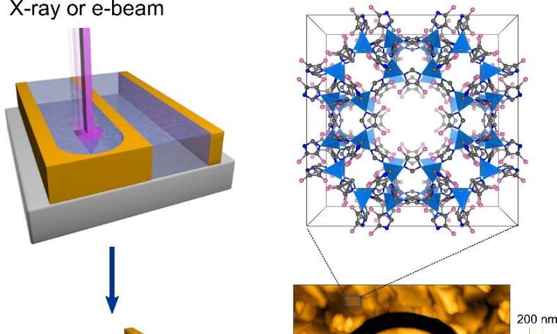
High-resolution lithography for nanoporous thin films

Researchers at KU Leuven (Belgium) developed a high-resolution lithography process to pattern metal-organic framework (MOF) films. This work, published in Nature Materials, will speed up the integration of these materials into microchips.
Metal-organic frameworks (MOFs) are molecular sponges that consist of organic molecules and metal ions. "There is a bright future for these materials in high-tech miniaturized devices such as low-power processors, resistive memory, sensors, and flexible electronics," says Professor Rob Ameloot from the KU Leuven Centre for Membrane Separations, Adsorption, Catalysis, and Spectroscopy (cMACS). "Both the MOF and microelectronics communities have been striving towards integrating MOFs in microchips, which requires two key engineering steps: thin film deposition and lithographic patterning."
In 2016, the group of Professor Ameloot developed , a method compatible with industrial chip fabrication. Now, the team takes one step further by realizing the direct lithography of MOF thin films with nanometer resolution. Conventional lithography techniques use a sacrificial layer, so-called photoresist, to transfer a pattern into the desired material. The use of photoresist complicates the process, and might induce contamination of the highly porous MOF films.

"Our goal was to eliminate the use of photoresist and still have high-quality MOF patterns." Says Min Tu, postdoctoral researcher at KU Leuven and first author of the paper. "Our method is based on selective X-ray or electron beam exposure of the MOF film, which induces chemical changes that enable its removal by a common solvent. This process completely avoids the resist layer, thus significantly simplifying patterning while maintaining the physicochemical properties patterned MOFs intact. Moreover, we can pattern much smaller features than previously possible, and our technique is already compatible with existing nanofabrication processes. To demonstrate some of the capabilities of this method, we fabricated a photonic sensor that responds to organic vapors. We are the first to realize the direct high-resolution lithography of these highly porous materials. We've found an exciting way to pattern MOF materials on surfaces. Now, it's time to design and implement them into miniaturized devices."
More information: Min Tu et al. Direct X-ray and electron-beam lithography of halogenated zeolitic imidazolate frameworks, Nature Materials (2020).
Journal information: Nature Materials
Provided by KU Leuven


